I just came across this video: https://www.youtube.com/watch?v=fxC5w3f8FkY which says that I can duplicate a trace on the bottom layer and then at the end just via it back up to increase the current capability of that trace.
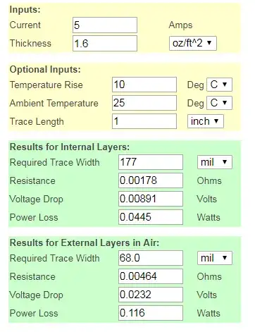
Say for example I want to carry approx 5A ish on a trace. A trace calculator gives me the following

I would require 68mm trace width. Is it possible to just do 34mm on the top layer and 34mm on the bottom layer? I.e each trace would be carrying approx 2.5A each. How would that work if the target device pin is SMD? I would need to via it up to the single 34mm trace, wouldn't that be a bottleneck?