0

Ideally a reference for small boards: The board that will be tested is 10 x 20 mm, and it's crowded. It doesn't have a lot of real estate left for test pads.

All I know is to look up IEEE papers:

The best resource so far, was an article in Printed Circuit Design & Fab, which recommends 0.9 to 1.0 mm test pads.


For this specific case, six signals will be exposed to the bed-of-nails: power, ground and four digital signals This is to be able to change firmware after the board has been assembled. Two of the digital signals are not exposed on any connectors.
adamaero
  • 677
  • 1
  • 7
  • 29
  • What are you trying to test on these boards? Or just general probe testing? – nate May 12 '20 at 18:34
  • "I need to expose six (6) signals to the bed-of-nails." and "pogo pins with 0.5mm pitch" @Nick Alexeev in EESE chat: https://chat.stackexchange.com/rooms/15/electrical-engineering – adamaero May 12 '20 at 18:37
  • Sometimes depending on manufacturing and test flow, you can use connector pads as test points prior to installing the connectors. Sometimes connectors are not installed during pick and place for one reason or another and in those cases the pads may be available for use as test points. – user57037 May 12 '20 at 19:10
  • @nate I need to expose power, ground, and four digital signals to be able to change firmware after the board has been assembled. Two of the digital signals aren't exposed on any connectors. – Nick Alexeev May 12 '20 at 21:27
  • Added info from comments - please always update question with added information. – Russell McMahon May 13 '20 at 04:11

1 Answers1

2

See 3.5.4.1 in IPC-2221A

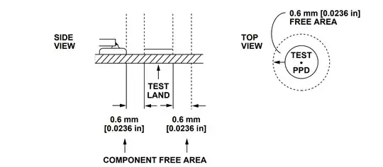
0.9mm is the smallest recommended but they say as small as 0.6mm is feasible in boards < 7700mm^2

Clearance required varies depending on adjacent component height (but minimum 0.6mm) and part height on probe side should not exceed 5.7mm.

enter image description here

Probe centers on 2.5mm grid if possible.

Spehro Pefhany
  • 397,265
  • 22
  • 337
  • 893
  • Thanks for the lead to the IPC standard. I've read the section 3.5 in the IPC-2221A. [I've got a 2003 edition.] They talk about SMT pads. They don't describe in detail how to use vias as test lands. They don't talk about the various pogo pin tip styles, and when to use which. Do you know if there's some other IPC standard which covers this in greater detail? – Nick Alexeev May 13 '20 at 00:38
  • @NickAlexeev no, sorry. There may be some info from the pogo pin manufacturers, but frankly all I've seen is dimensional drawings- it's fairly obvious that you'd use conical ones for holes, inverse conical for through-hole leads and pointy ones for pads but the details seem left up to the user to figure out. There may be an ecosystem of information for the folks who design test fixtures and so on. Years ago I had a subscription to a US magazine aimed at test engineers but the postal regulations changed so it was no longer practical to send those out for free. – Spehro Pefhany May 13 '20 at 05:12