2

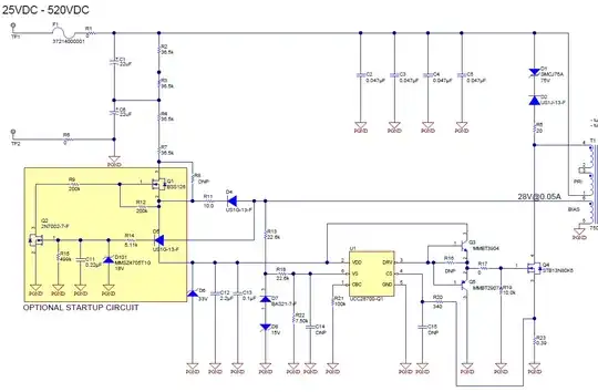
In the circuit below, how is Q1 turned on? When there's voltage in the bias winding, it turns Q2 On and subsequently turns Q1 off. Also, does the end of R4+R7 keep floating when Q1 is off? It should go to ground. I'd appreciate any help to better understand the startup circuit in the yellow square.

enter image description here

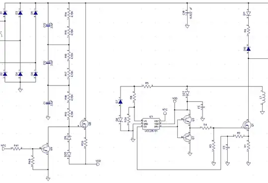
EDIT: Idea with an Enhancement MOSFET

enter image description here

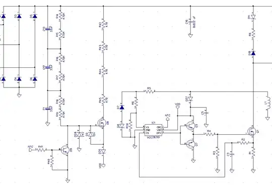
EDIT: Another approach with Enhancement MOSFET
enter image description here

  • 1
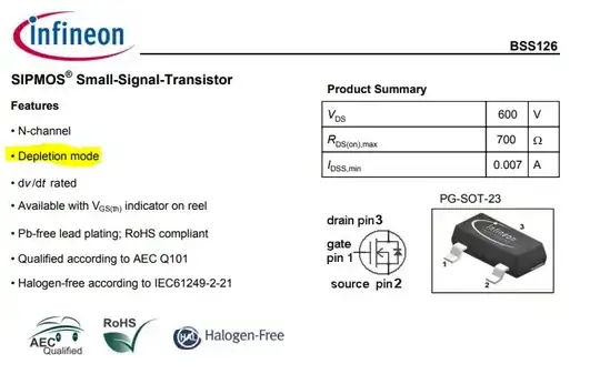
    Note that depletion mode FETS are not quite as rare as hens teeth, but getting that way. BSS126 datasheet . The clue here that it is a depletion mode device is that the source sits at about +28V (via D4) and the gate is at Vs when Q2 is off and at Vs/2 when Q2 is on (so at about -14V negative bias relative to source.) || ... – Russell McMahon Jun 02 '20 at 02:21
  • ... Digikey's depletion mode listings - 270 line items (many duplicates) here – Russell McMahon Jun 02 '20 at 02:22
  • @RussellMcMahon Can you check the circuit I added using an enhancement MOSFET? The idea is to have a known current to charge the Vdd capacitor. When the controller starts, CBC/NTC pin is a current source I'm using for the BJT to turn off the FET. –  Jun 02 '20 at 02:56
  • No! - I can see your thought processes but that cicruit would be fatal In CCT1 (original) the series resistor string provides the power up Vdd and it is turned off once the converter provides 28V directly. | In CCT2 you are using the balanced series string to turn on the enhancement mode FET (OK enough) BUT the FET supplies Vdd directly from Vhv. This state is terminated by NTC going high (IC1 pin 1) BUT there is no reason to expect that Vdd will not rise to about Vhv before this happens. | – Russell McMahon Jun 02 '20 at 07:11
  • Your series resistor string needs to be in Q8 drain and needs a seperate gate drive resistor (can be very high R) and the drain needs a clamp zener (D9 does this here but cct is being changed) (provided in CCT1 via the initially on FET) . The gate also needs clamping to < Vgsmax. | SO fatally flawed as is BUT not too hard to fix it. – Russell McMahon Jun 02 '20 at 07:11
  • @RussellMcMahon Could you check the other option I just added? In the previous one I had a known charging current limited by the source resistor, however in the new one the current is not constant, I think. –  Jun 02 '20 at 12:50
  • True re source resistor in 2nd cct - but FET will dissipate the majority of the voltage drop - resistors are a better choice (usually). I won't go over it again as the 3rd cct is potentially better. || 2nd and 3rd cct both have the fixable problem that NTC is asserted to turn off Q8 once Vdd is provided BUT Vdd is initially provided via Q8 so it will "hiccup" and may or may not start the smps. This is fixable by driving NTC from a voltage derived from L1. Either add another diode between D27 cathode and Vdd or provide a separate diode and cap and ... from L1. ... – Russell McMahon Jun 03 '20 at 01:50
  • Having Vdd 1 diode drop under D27 cathode should not cause problems. || I strongly recommend a zener across R3 or where R3 is. The function of R3 is uncertain. Zener voltage is slightly above Vdd max and clamps Millar capacitance coupling from drain. Mount zener as close to FET gs as reasonably possible. If load is entirely non inductive always then zener is notionally not needed - but Murphy can always manage it :-). – Russell McMahon Jun 03 '20 at 01:54
  • @RussellMcMahon many thanks, I will fix 3rd cct as per your suggestion. One last question before closing the topic. In 2nd cct I have a known current to charge the cap due to the source resistor. This is regardless the input voltage. But in 3rd cct, how do I know the current I will have to charge the controller cap? In this case I'll have a voltage drop on the drain resistors compared to the 2nd cct where drain is directly connected to the bus. I will simulate it, but I want to know how to calculate it. Then if I know the current, I know the startup time using the charge formula. –  Jun 03 '20 at 02:08
  • You can still use a source resistor to control charge current while using draim resistors to drop most of voltage. If Rdrain x Iconstant is somewhat less than Vhv/Rdrain thn the FET will drop the balance of the voltage in to make it work as constant current charge. I'd not have thought that startup time was TOO critical . Vhv probably rises relatively fast and current tends then to be ~~= (Vhv-Vdd)/Rdrain. As soon as the smps starts it takes over. – Russell McMahon Jun 03 '20 at 03:35
  • I haven't looked at the controller data sheet but they often have a Vstart and a lower Vrun_min so you can charge C5 as slowly as you like - when it reaches Vstart the smps runs on the cap and needs to start and self power before the cap voltage reaches Vmin. This allows you to have a very low dissipation start up resistor chain and it can even be designed to not need to ever turn off. – Russell McMahon Jun 03 '20 at 03:35
  • Your IC datasheet here does as above see P5 section 7.5 . Start voltage is ~= 21 V and lockout Voltage is 8V. Rgei example circuit shows s single start resistore from Vhv which is NOT turned off when the smps starts. Dissipation can be low as the run cp can be trickled up slowly until the smps starts. The cap has to be large enough to power it while starting. – Russell McMahon Jun 03 '20 at 03:41

1 Answers1

2

Q1 is a depletion mode device, therefore it is ON with zero Vgs. When Vin is applied, Q2 is off, Vgs of Q1 is held to zero by R12, and Zener D6 clamps the voltage to the controller to ~33V.

enter image description here

The controller starts switching, causing the bias winding to deliver energy to the Vdd input of the controller through D4, and to the gate of Q2 through D6.

Q2 pulls the gate of Q1 below the source, turning Q1 off, and therefore eliminating the power dissipation in the startup circuit.

The 200K voltage divider on the gate of Q1 prevents damage from exceeding the +/-20V max Vgs rating of the device.

John D
  • 23,824
  • 1
  • 41
  • 61
  • But if R4 & R7 is not pulled down to ground, doesn't this cause the input capacitors to unbalance? –  Jun 02 '20 at 01:56
  • @Blue_Electronx Yes, it would. I would have not connected the midpoint of the caps to the startup string, and would have used separate balancing resistors on the caps. It might still be OK depending on the voltage ratings of the caps, but good catch. – John D Jun 02 '20 at 02:08
  • I have edited the post and added an idea using an enhancement MOSFET. What do you think? The plan is to have a known current to charge the Vdd capacitor. When the controller starts, CBC/NTC pin is a current source I'm using for the BJT to turn off the FET. –  Jun 02 '20 at 02:53