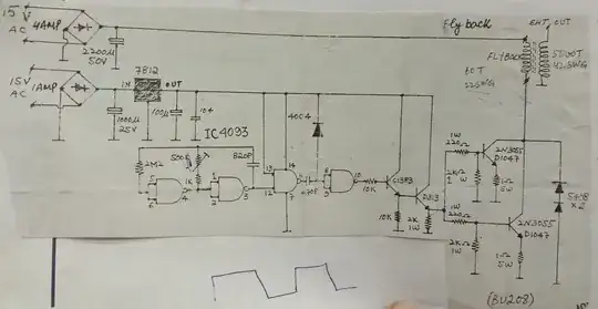
In this circuit can any one tell me complete working of ic cd 4093. Mean how schmitt triggering occur in this circuit?
And how to draw square wave in different steps of gates? What is the purpose of transisters in this circuit??
I will be thank full ....

- 1
- 1
-
1Complete working of CD4093 – Andy aka Dec 12 '20 at 16:52
1 Answers
The two left gates from your 4093 are just used as inverters. The feedback through the 820 pF capacitor¹ and the resistors form a delay, so that your adjustable resistor allows you to adjust the frequency at which the output of the second gate toggles.
This is just a poor man's oscillator from the 1970's.
Schmitt triggering really doesn't matter much here (it makes things a bit more noise-resistant, but I don't see how this would be a significant problem here). It happens within the inputs of all four NAND gates.
You'd not build anything like this in 2020. The oscillator is the least of the obsolete things here – the bad regulation and high amount of waste heat in the rightmost two NPN transistors is really what makes this schematic so obsolete.
A modern solution to the same problem would be to employ dedicated flyback controllers, or at least a dedicated PWM controller that has some feedback loop bandwidth compensation, and to use better switching transistors.
¹ all these components should have names like "C1" or "C2"... This is not a great schematic.
- 94,373
- 5
- 139
- 252
-
-
That's the central part of a flyback switcher? The switch... You might want to read what a flyback power supply does. – Marcus Müller Dec 21 '20 at 11:30