Not notoriously trivial because the reason is notoriously silly.
Benjamin Franklin did not know what actually moved to carry electricity so had to guess a polarity for each charged component.
He guessed wrong but by the time we figured out it was the negative-assigned particle (electrons) that actually moved, it was too ingrained and difficult to change so most things continue to use so-called "conventional" current flow, not actual electron flow.
That is an N-channel JFET which looks like this:

https://www.tutorialspoint.com/basic_electronics/basic_electronics_jfet.htm
Note the P and N-doped silicon. That forms a diode. If your gate voltage is more positive than the source terminal, that forward biases the diode and produces a short which blows the JFET.
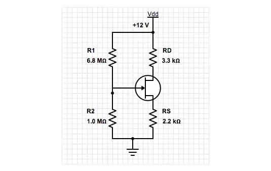
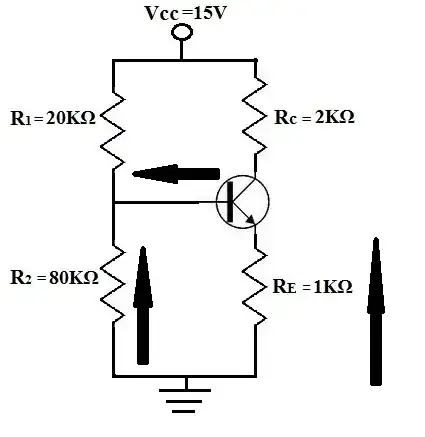
So an N-channel JFET must have a gate voltage that is more negative than the source so that the PN-junction is reverse biased. In your circuit, the way the voltage dividers and resistors are set up, the gate voltage is lower than the source pin voltage, even though both voltages are still positive when measured relative to GND. Also, unlike the JFET circuit, the PN junction in the BJT is forward biased and heavily influences what voltage will appear between R1 and R2 since it effectively puts a diode and Re in parallel with R2.
It is not obvious in your diagram because it is using a single supply and dividers. It is much more obvious in a diagram like this:

https://www.tutorialspoint.com/basic_electronics/basic_electronics_jfet.htm
 a simple voltage divider JFET. Assuming these authors are following the same conventional current rules in all other circuits, here, the Gate-source voltage should be positive, as just like v_be, but this time it is negative. why?

