0

The following code is given. My task involves drawing a visual hardware representation that outlines the modules, their associated ports, and the interconnecting signals. Check out my solution below. Am I on the right track?

flipflop.vhdl:

library ieee;
use ieee.std_logic_1164.all;

entity Clocked_Logic is

port (i_Clk      : in  std_logic;
      i_Switch_1 : in  std_logic;
      o_LED_1    : out std_logic);

end entity Clocked_Logic;

architecture RTL of Clocked_Logic is

signal r_Switch_1 : std_logic := '0';
signal r_LED_1    : std_logic := '0';

begin

    -- this clocked-sequential process starts when i_Clk state change
    -- the sensitivity list contains only i_Clk
    p_Register: process (i_Clk) is
    begin

        if rising_edge(i_Clk) then

            r_Switch_1 <= i_Switch_1;

            if i_Switch_1  = '0' and r_Switch_1 = '1' then 

                r_LED_1 <= not r_LED_1;

            end if; 

        end if;

    end process p_Register;

    o_LED_1 <= r_LED_1;

end architecture RTL;

My solution:
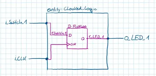
enter image description here

  • 1
    https://electronics.stackexchange.com/questions/13995/how-can-i-generate-a-schematic-block-diagram-image-file-from-verilog/269121 <-- the same from verilog. You can possibly read simple VHDL nowadays directly with yosys, or you can convert using ghdl – Marcus Müller Nov 28 '23 at 20:11

2 Answers2

2

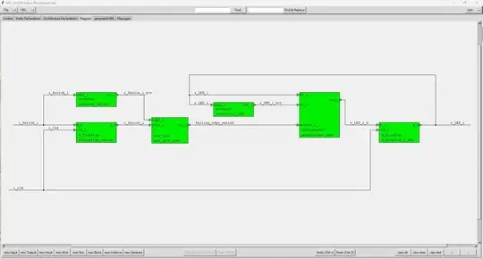
Your design has 2 flipflops. The first flipflop is needed to store r_switch_1. The second flipflop is needed to store r_LED_1. The second flipflop will toogle as soon as there is a falling edge at i_Switch_1. A toogle flipflop can be build by a multiplexer which leads the q-output of the flipflop back to the d-input of the flipflop, in one case as a inverted signal and in the other case as a not inverted signal. This results in a schematic like this: enter image description here

1

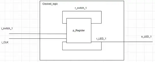
I think you are not totally correct. Your code is not only a DFF. Your p_Register process also has some logic.

It seems that it needs r_switch_1 to perform a "AND" with i_switch_1, so the process needs both signals as inputs. Also inside the if, the process needs to know the logic state of r_LED_1. So it is a input of your process as well.

That means that r_switch_1 and r_LED_1 need to loopback to the p_Register process.

enter image description here

vivier
  • 597
  • 15
  • Tanks a lot. Does the symbol <= from the line r_Switch_1 <= i_Switch_1; means a register? So with this line I am creating a flipflop right? – Marco Moldenhauer Nov 29 '23 at 10:51
  • 1
    Yes that line synchronize the input signal with the clock, it is a DFF. The schematic proposed is the outside representation of your module. In reality the hardware description of p_Register will contain at least one DFF. – vivier Nov 29 '23 at 12:35