0

Content is from the book Design of Analog CMOS Integrated Circuits (https://electrovolt.ir/wp-content/uploads/2014/08/Design-of-Analog-CMOS-Integrated-Circuit-2nd-Edition-ElectroVolt.ir_.pdf) on Page 112.

Due to a manufacturing error, in the circuit of Fig. 4.19, \$M_2\$ is twice as wide as \$M_1\$. Calculate the small-signal gain if the DC levels of \$V_{in1}\$ and \$V_{in2}\$ are equal.

enter image description here

The following is my analysis. Since it's symmetrical, we can use virtual ground to analyze this circuit:

enter image description here

First, we only analyze the left part with KCL:

$$ -\frac{V_{out2}} {R_D} = V_{in} g_{m1} + \frac{V_{out2}} {r_{o1}}$$ $$\Rightarrow \frac{V_{out2}} {V_{in}} = -g_{m1} (R_D \parallel r_{o1})$$

Now we only analyze the right part with KCL:

$$ -\frac{V_{out1}} {R_D} = -V_{in} g_{m2} + \frac{V_{out1}} {r_{o2}}$$ $$\Rightarrow \frac{V_{out1}} {V_{in}} = g_{m2} (R_D \parallel r_{o2})$$

We combine this two equation into one:

$$\frac {V_{out2} - V_{out1}} {2 V_{in}} = -\frac{1}{2} (g_{m1} + g_{m2}) R_D$$

Since \$g_{m2} = 2 g_{m1}\$ $$\frac {V_{out2} - V_{out1}} {2 V_{in}} = -\frac{3}{2} g_{m1} R_D$$

But the book said:

$$|A_v| = \frac{2 R_D} {1/g_{m1} + 1/ g_{m2}} $$ $$|A_v| = \frac{4} {3} g_{m1} R_D$$

JYelton
  • 34,119
  • 33
  • 145
  • 265
kile
  • 798
  • 2
  • 11
  • Your calculation seems correct but the result is wrong because you cannot split the circuit like that as it's not symetric. The voltage vgs of M1, M2 in this case are not same magnitude as you drew. – internet Dec 16 '23 at 12:19
  • @internet What should you use to analyse this circuit? – kile Dec 16 '23 at 13:48
  • You can always draw the small signal model to calculate gain but for this circuit I can do it in my head. Assume that you use T model for the mosfets and ignore the output impedance. id1 = (Vin1 - Vin2)/(1/gm1 + 1/gm2) Vout = Vout1 - Vout2 = id1*RD - (-id1)*RD = 2id1*RD = 2RD(Vin1 - Vin2)/(1/gm1 + 1/gm2) So Vout/(Vin1-Vin2) = 2RD/(1/gm1 + 1/gm2) = 4/3*gm1*RD with gm2 = 2*gm1 – internet Dec 16 '23 at 14:00
  • @internet Could you please show me the small signal circuit diagram to make it easier to understand you equation? – kile Dec 16 '23 at 15:04
  • check this: https://yourimageshare.com/ib/fqwo6Yy3wO – internet Dec 16 '23 at 15:18
  • I also prefer the T-model. https://electronics.stackexchange.com/questions/536586/why-does-a-circuit-model-of-n-mosfet-exhibit-a-finite-resistance-between-source/536639#536639 Using it we can see by inspection that the asymmetrical voltage gain is RD/(1/gm1 + 1/gm2), and if gm2 = 2*gm2 we have 2/3gm1RD Thus, for differential output (Vout1 - Vout2) the gain will be twice this value the value 4/3gm1RD – G36 Dec 16 '23 at 15:21
  • @G36 Is symmetrical valid in this case? – kile Dec 16 '23 at 15:23
  • Do you have in mind your method (grounding the M1 and M2 source)? – G36 Dec 16 '23 at 15:25
  • @G36 the source of M1 and M2 are virtual grounded if it's symmetrical. – kile Dec 16 '23 at 15:32
  • But this is not the case here. We do not have virtual GND because gm1 is not equal to gm2. So the middle point will not be at 0V. And this is why your method does not give the correct result. Using your method we have the M1 gain RD/(1/gm1) and M2 gain is RD/(2 * gm1) and the overall differential gain is 3gm1RD – G36 Dec 16 '23 at 15:43
  • That's a bizarre manufacturing error. I know it's just a textbook example but I'm struggling to imagine how any problems at the manufacturing stage could alter the width of one transistor and not another! – Hearth Dec 16 '23 at 17:50
  • @internet Could you please have a look at my answer. What's wrong here? – kile Dec 17 '23 at 23:06
  • @G36 Could you please have a look at my answer. What's wrong here? – kile Dec 17 '23 at 23:07

1 Answers1

0

The following is my analysis.

enter image description here

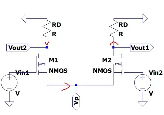
Firstly, we analyse the left part of this circuit with the use of KCL.

$$- \frac{V_{out2}} {R_D} = (V_{in1} - V_p) g_{m1} + \frac{V_{out2} -V_p} {r_{o1}}$$

$$\Rightarrow - V_{out2} (\frac{1} {r_{o1}} + \frac{1} {R_D}) = V_{in1} g_{m1} - V_p (g_{m1} + \frac{1} {r_{o1}})$$

$$\Rightarrow V_p = \frac{V_{in1} g_{m1} + V_{out2} (\frac{1} {r_{o1}} + \frac{1} {R_D})} {g_{m1} + \frac{1} {r_{o1}}}$$

Secondly, we analyse the right part of this circuit with the use of KCL.

$$ \frac{V_{out1}} {R_D} = -(V_{in2} - V_p) g_{m2} + \frac{V_p -V_{out1}} {r_{o2}}$$

$$\Rightarrow V_{out1} (\frac{1} {r_{o1}} + \frac{1} {R_D}) = - V_{in2} g_{m2} + V_p (g_{m2} + \frac{1} {r_{o2}})$$

We could substitute \$\frac{V_{in1} g_{m1} + V_{out2} (\frac{1} {r_{o1}} + \frac{1} {R_D})} {g_{m2} + \frac{1} {r_{o2}}}\$ for \$V_p\$ from what we previously got.

$$\Rightarrow V_{out1} (\frac{1} {r_{o1}} + \frac{1} {R_D}) = - V_{in2} g_{m2} + \frac{V_{in1} g_{m1} + V_{out2} (\frac{1} {r_{o1}} + \frac{1} {R_D})} {g_{m1} + \frac{1} {r_{o1}}} (g_{m2} + \frac{1} {r_{o2}})$$

Since we already assume \$g_{m1} r_{o1} \gg 1\$ and \$g_{m2} r_{o2} \gg 1\$

$$\Rightarrow V_{out1} (\frac{1} {r_{o1}} + \frac{1} {R_D}) = - V_{in2} g_{m2} + \frac{V_{in1} g_{m1} + V_{out2} (\frac{1} {r_{o1}} + \frac{1} {R_D})} {g_{m1}} (g_{m2})$$

$$\Rightarrow V_{out1} (\frac{1} {r_{o1}} + \frac{1} {R_D}) = - V_{in2} g_{m2} + V_{in1} g_{m2} + V_{out2} (\frac{1} {r_{o1}} + \frac{1} {R_D}) \frac{g_{m2}} {g_{m1}}$$

$$\Rightarrow V_{out1} (\frac{1} {r_{o1}} + \frac{1} {R_D}) - V_{out2} (\frac{1} {r_{o1}} + \frac{1} {R_D}) \frac{g_{m2}} {g_{m1}}= V_{in1} g_{m2} - V_{in2} g_{m2} $$

We also assume \$r_{o1} \gg R_D\$ and \$r_{o2} \gg R_D \$

$$\Rightarrow V_{out1} (\frac{1} {R_D}) - V_{out2} (\frac{1} {R_D}) \frac{g_{m2}} {g_{m1}}= V_{in1} g_{m2} - V_{in2} g_{m2} $$

$$\Rightarrow (\frac{1} {R_D}) (V_{out1} - V_{out2} \frac{g_{m2}} {g_{m1}}) = V_{in1} g_{m2} - V_{in2} g_{m2} $$

For third equation.

$$- \frac{V_{out2}} {R_D} = \frac{V_{out1}} {R_D}$$

$$\Rightarrow - V_{out2} = V_{out1} $$

Substitute \$-V_{out2}\$ for \$V_{out1}\$

$$\Rightarrow (-\frac{1} {R_D}) V_{out2} (1 + \frac{g_{m2}} {g_{m1}}) = g_{m2} (V_{in1} - V_{in2}) $$

The gain will be

$$\frac{V_{out2} - V_{out1}} {V_{in1} - V_{in2}} = \frac{2 V_{out2}} {V_{in1} - V_{in2}} = \frac{2 g_{m2}} {-\frac{1} {R_D} (1 + \frac{g_{m2}} {g_{m1}})} $$

$$\frac{V_{out2} - V_{out1}} {V_{in1} - V_{in2}} = - \frac{2 R_D g_{m2}} {(1 + \frac{g_{m2}} {g_{m1}})} $$

As we all know \$g_{m2} = 2 g_{m1}\$

$$\frac{V_{out2} - V_{out1}} {V_{in1} - V_{in2}} = - \frac{2 R_D g_{m2}} {(1 + 2)} =- \frac{4 R_D g_{m1}} {3} $$

kile
  • 798
  • 2
  • 11
  • @internet Could you please have a look at my answer. What's wrong here? – kile Dec 17 '23 at 16:21
  • @G36 Could you please have a look at my answer. What's wrong here? – kile Dec 17 '23 at 16:21
  • @Hearth Could you please have a look at my analysis? – kile Dec 17 '23 at 16:43
  • Hi @kile, I only came across this by chance--you can't @-ping someone who hasn't already commented on the same post, so none of us got notifications for this. I'm afraid I don't have the energy or focus to go through this analysis on my day off, though. – Hearth Dec 17 '23 at 20:18
  • It would be much simpler if you ignore ro1, ro2 at the beginning. I haven't checked your equations but if you need to solve for the general cases, you should write one more KCL equation at node Vp. So now, you would have three equations and three variables Vp, Vout1, Vout2 to solve. – internet Dec 17 '23 at 23:41
  • @internet Why would I need third equation? There is only one unknown variable $V_p$? What's the third equation look like? – kile Dec 18 '23 at 08:32
  • We need three equations because we have three unknowns. You cannot solve it using only two. – G36 Dec 18 '23 at 14:34
  • @G36 Please take a look at my equation – kile Dec 18 '23 at 20:41