Assuming this is a one-off...
Let's compare two cases...
500 buttons in 2ms = 250 kbps
500 daisy chained boards
Implementation would be something like a shift register, either in hardware or with a micro. With a clock buffer and a 1-bit latching shift register on each board there should be no signal integrity issues because signals are only transmitted to the next board, so you could use fast clock speeds. No problem to reach the target update speed.
- 5 wire cables: Latch, Data, Clock, VCC, GND
You need 499 identical cables (998 connectors). So the only practical solutions are either to whip an unpaid intern into making them or buying them pre-made. This restricts the choice to off the shelf cheap with 5 (or more) wires... maybe RJ45 or JST/0.1" jumpers...
- 4 wire cables: Data, Clock, VCC, GND
To have a wider choice of cheap readymade cables, 4 wires would be more practical as it allows using RJ11, maybe even USB cables.
This means the latch signal should be encoded with the clock. No clock for a while means latch in the button data, then pulsing the clock shifts the data bits.
It should be possible to do that with a 74HC74 plus a bunch of passives and careful engineering of the clock signal, or a cheap micro on each switch PCB. The latter can also allow debouncing locally, but you have to whip an unpaid intern into programming 500 mcu's or buy them pre-programmed.
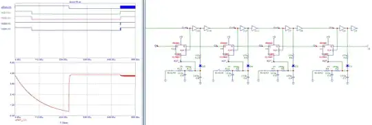
Here's a quick and dirty example. Each button PCB has a buffer (two inverters) and a D flip flop. The switches are filtered by 100nF capacitors.
Initially, all the flip flops are set to 1. First the clock is held high for 250µs, which sends low voltage to the diodes. When the switch is on, it discharges the 100pF cap, which resets the flip flop. Then clock goes low for another 250µs, which brings the reset lines high again through the diodes. Then 500 clock pulses are emitted at 1MHz, which shifts all the data through the flip flops: the result is inverted, closed switches result in a 0 bit. The last flip flop in the chain has its input tied to VCC, so as the whole shift register is read, it is filled with 1's at the same time. Then the cycle repeats.
I used high value resistors because the per-PCB consumption should be kept low.
- 3 wire cables: Data, VCC, GND
With MCUs this is also possible by encoding the data into the length of a pulse. The last MCU in the chain sends its status every 2ms, then each MCU acts as a repeater and adds its own button status as the end of the pulse train. Decoding could will probably require a dedicated bitbanging micro, or a fast micro using oversampling. But you can use 3.5mm jack cables (and their legendary reliability).
63 daisy chained boards
The alternative is to use one "smart" board for every 8 buttons for example. This adds more 2-wire cabling between buttons and board, and it reduces the number of multiwire cables between boards.
This may be an advantageous solution if it is easier and cheaper to find a large number of 2-wire cables, than a large number of 4-5-wire cables.
In this case each board would either use a 74HC165 shift register, or a microcontroller with local debouncing.
In all cases, wires will be long and thin so each board should use minimum power.

