5

I'm working on a CubeSat project and I need to produce a 3.3 V voltage rail for an ADC (ADC128S102). The ADC only needs 3 mA total when in active mode. I'm selectively upgrading the most critical parts on the bus to versions that are radiation tolerant/hardened.

I have a +5 V rail and I want to avoid buying another voltage regulator just to produce this 3.3 V line if I can. I have an unused op-amp (OPA4H199-SEP) that I think I could use to produce a 3.3 V line for the ADC. This 3.3 V is only used for the digital signals reference, not the analog reference voltage itself.

The ADC needs 0.1 μF + 1 μF of decoupling on the digital line and I simulated the op-amp feeding these capacitors and it looks like an isolation resistor of 100 Ω makes the op-amp stable.

If the ADC drew its maximum rated current from this supply constantly, the voltage would drop to 3.0 V on the digital input of the ADC. This is still within the operating conditions of the part and seems like it would still produce valid logic levels for an MCU to read.

Is there any reason that this wouldn't work in practice or wouldn't behave like I've simulated? I know op-amps could be used to drive the base/gate of a transistor to produce a linear regulator, but based on everything here, it looks like I can get away with just using the op-amp to drive it directly.

The circuit would probably look something like this (with the +5 V line replaced with a +10 V line):

schematic

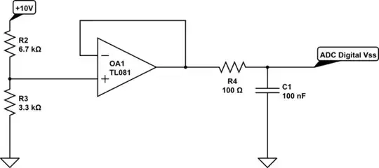
simulate this circuit – Schematic created using CircuitLab

ocrdu
  • 9,195
  • 22
  • 32
  • 42
cEEa
  • 473
  • 2
  • 11
  • 3
    Note: You are effectively using the op-amp as a linear voltage regulator, and like any linear regulator, it will waste power, and make heat. If it supplies 3mA to the ADC, then it must draw at least 3mA from the 5V supply. That means, the op-amp is "dropping" 1.7V. That means, it's dissipating at least 5.1 milliwatts. (1.7*3=5.1) Is that a bad thing? Maybe, maybe not. It's your power budget, your thermal budget. Only you can say. – Solomon Slow Jan 12 '24 at 15:07
  • Yes this is something I've kept in mind. 5.1 mW is relatively minor both from a power and thermal perspective for the application I'm working on. – cEEa Jan 15 '24 at 01:51

7 Answers7

9

Here's a fragment snipped from the schematic of an actual spaceflight instrument (NICER), using an opamp as a low current voltage regulator. Basically take DC feedback from the the output RC, but leading AC from inside it. The C8*R18 time constant should be a few times the C16*R17 time constant for good stability.

enter image description here

John Doty
  • 4,304
  • 1
  • 9
  • 17
  • Thanks for the actual schematic. I simulated this one as well and it behaves nicely in the actual circuit. Any thoughts on this versus the currently accepted solution? The currently accepted solution has a lower part count but takes longer to reach a stable voltage due to the large bulk capacitance of the snubber cap. – cEEa Jan 11 '24 at 20:56
  • @cEEa Your call. I have a slight preference for MLCCs over tantalums, as I think them more reliable (but I've flown lots of tantalums). – John Doty Jan 11 '24 at 21:23
  • @cEEa both the snubber and this - "in-the-loop" compensation are valid approaches to stabilize capacitive drive. The snubber has better load regulation. The components here are usually small and cheap whereas the components for the snubber can be a bit larger. The snubber usually provides lower supply impedance however, and lower part count. – tobalt Jan 12 '24 at 06:30
  • @JohnDoty nothing forbids building the snubber with MLCC :) Although I'm curious: aren't the large temperature differences encountered in space not a severe reliability issue for MLCC due to stress cracking? – tobalt Jan 12 '24 at 06:48
  • @tobalt Yes, but if you make a snubber with an MLCC you need an extra resistor so the component count advantage of the snubber approach goes away. – John Doty Jan 12 '24 at 11:56
  • @tobalt In LEO, things on the outside of your spacecraft, like solar panels, suffer wild temperature swings as the spacecraft goes into and out of eclipse. But inside, the temperature swings are usually pretty mild. – John Doty Jan 12 '24 at 12:04
3

Is there any reason that this wouldn't work in practice or wouldn't behave like I've simulated? I know op amps could be used to drive the base/gate of a transistor to produce a linear regulator, but based on everything here, it looks like I can get away with just using the op-amp to drive it directly.

While an opamp is better than a resistive bridge, it can also inject some noise into the ADC rail. It also depends on how accurate you need the

You would get approximately 10nV/sqrt(Hz) so over 16kHz (bandwidth of RC) you would be 126sqrt(Hz)*10nV/sqrt(Hz) = 1260nVrms of noise. with a PSRR of ADC128S102). There isn't a PSRR figure in the document so I'm unable to coment on that.

Other than that I would probably reduce the voltage drop across "R4" and lower that to as little as possible as if the ADC current is not constant you could get issues with voltage drop across it. That being said don't exceed the capacitance of the OP4H199. Including R4 in the feedback loop could help, but could also introduce instability so look at the AC response.

Voltage Spike
  • 82,181
  • 41
  • 84
  • 220
  • This rail is only used for the digital side of the ADC. I'm using a separate precision 5V line for the actual analog comparison. – cEEa Jan 11 '24 at 20:20
3

Yes that works well. I do the same often.

Instead of the series resistor (which strongly impacts regulation as you noticed), one can place a parallel snubber, to make the opamp stable despite the capacitive load. The snubber makes the load become resistive at the frequency of the oscillation, thus quenching it.

Al electrolytic caps are perfect snubbers as shown in this answer, but might not work well in space due to vacuum. In that case you can use a Tantalum cap or a large MLCC with a suitable resistor instead. The linked answer contains a simulation.

tobalt
  • 21,701
  • 22
  • 90
  • 1
    Thanks for the link, that seems like a good approach. I already have a Tantalum cap on the board with 68 uF and .250 ESR and it looks like it solves any stability issues in the simulation. – cEEa Jan 11 '24 at 20:47
2

You could try including R4 in the feedback path (connect the inverting input after R4), that would keep the output voltage at 3.3 V. You'd need to check stability and performance to see how those are affected.

GodJihyo
  • 22,826
  • 1
  • 20
  • 58
  • +1 to this. At 3mA load, your output will sag 300mV with the original setup. Note that 100Ω and 1.1μF gives you a pole at about 1.44kHz, so that will limit your transient response, but not worse than just putting a resistor in series with the output. – mapplejacks Jan 11 '24 at 19:27
  • Taking feedback from after the resistor will change nothing. It will only slightly add the open loop output impedance of the opamp. To make it work you'd need the full compensation scheme as shown by John Doty. – tobalt Jan 12 '24 at 06:50
0

If the ADC uses a voltage reference then you may find that this works well, but if it’s trying to perform successive approximation using the supply as a reference then you can expect bad behaviour resulting in the low-order bits being unreliable. Its worth prototyping if you have the opportunity to do so.

Frog
  • 7,287
  • 1
  • 9
  • 13
0

From the first page of the datasheet of your ADC : enter image description here

VA (the analog power supply) is directly used as reference voltage for the ADC, this means :

  • your full scale is dependent of the exact VA voltage
  • any change in VA means a change in your reading
  • any noise on VA will be noise on your reading

Also note that the current consumption of 3mA (no idea where you got that value, maybe the 3.1mA for the total consumption of analog + digital) is probably just a typical or maximal value, so it might change in time and depending on other things like temperature.

So all depends on the accuracy you need. If you can live with +-20% on your readings, then it will probably work.

With calibration, you might be able to get down to 5-10% (but I'm not sure how well you can calibrate for space temperature/pressure).

If you want anything halfway precise, either get yourself an ADC with internal reference, or use a linear voltage regulator : it's just a 3 pin component, and given that you have only 1.7V difference between your 5V input and 3.3V output, and that your current is <3mA, it will not waste much power (and certainly less than with your OP-AMP)

Sandro
  • 7,277
  • 11
  • 37
  • 1
    I have a precision 5 V reference that is used for the VA input of the ADC. It's a separate line from this 3.3 V line that is for VD, which is the one I'm trying to generate from the op amp. The 3.1 mA is the total consumption of analog + digital – cEEa Jan 11 '24 at 20:18
0

I would recommend just using a voltage regulator. For 3mA an SOT23 version will do. Smaller and up to the job.

user242579
  • 371
  • 1
  • 4
  • I think the challenge for this design is that it is for a CubeSat, and therefore the integrated circuits need to be radiation tolerant/hardened. – Chester Gillon Jan 12 '24 at 21:59