Most of the information can be found in "The Art of Electronics" by Horowitz and Hill
In order to understand transistor response time it is required to understand the next:
Storage time (ts): the time the transistor requires in order to come out of saturation. i.e. when the transistor is saturated it contains a certain deposit of charge that takes time to be depleted. If you place an oscilloscope comparing a step drop at the input with your output you will notice a time the output does not even start to rise, that is mainly the time the transistor is depleting its charge (ts)
Ccb: capacitance between collector and base. Although there are other parasitic capacitance at the transistor this is the most influential one. you should find this value in all the transistors datasheets. The smaller the value the better the response time of the transistor.
Ignoring the ts for a second lets assume R3, Ccb and Cl (load capacitance you did not include in your schematic) is relatively big. the collector rise will look exponential due to these component combination and the rise time (10-90%) will be approximately:
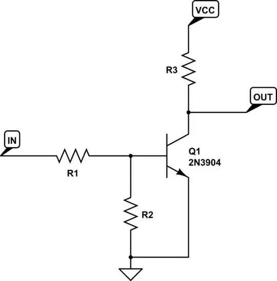
2.2*R3*(Cl + Ccb)
If on the other hand these values are quite small that still doesn’t mean the rise will be a step. In that case the phenomenon that will dominate the rise will be that the current through Ccb will act as a negative feedback to the base that will limit the rise and instead of an exponential rise you will get a ramp
In essence, many square wave response will start as a ramp and end up as exponential. The way to make a prediction about the rise time is first to determine the point where the rise is turning from a ramp to exponential via the next formula:
VX = Vcc - Rc * ((Vbe - Vin(low) / Rs ) + Cl*(dVc/dt))
while:
dVc/dt = (Vbe - Vin(low))/(Ccb*Rs)
In your circuit:
Rs = R1 || R2
Vbe = 0.7V (basically)
Vin = if other than 0V use Thevenin to calculate
If that value is negative the rise is entirely exponential and the rise time (10-90%) can be derived from:
2.2*R3*(Cl + Ccb)
Else calculate the time the ramp (dVc/dt) will reach Vx and add to it the time from Vx to the 90% reach using the exponential formula
as for the fall time you can use the next formulas:
-dVc/dt = ( 1 / (Cl + (Hfe + 1)*Ccb) * ( Hfe * ((Vin(high) - Vbe)/ Rs) - (Vcc - Vc)/Rc)
Tf = 0.8*Vcc / (dVc/dt)
Note that at the first formula Vc can be sometimes negligible and can be discarded, otherwise, you will need to calculate it in several steps to get a good estimate
Other notes:
Hfe is relative to your signal frequency and you should derive the correct value from the datasheet
Storage time: although this is a value that is related to the transistor, there are methods to lower its effect. Look for "Baker clamp" and "speedup capacitor" on that.
These are crude estimates and should be backed up (datasheet graphs, SPICE and actual testing's)