0

When making chips using lithographic techniques, How are the transistors and capacitors and other components "printed" onto the board?

When we print one we use things like UV or E-beam to print out the shape we want (using some kind of mask), but after we're left with the desired shape, how are the transistors, capacitors, resistors (and so on) placed? Are they there all along somehow?

I bet this question has a simple answer but I must be mis-interpreting some concept which doesn't let me understand.

2 Answers2

2

With the different masks you can in 2D decide what pattern you want where on the chip. Transistors are nothing more than a few regions on the silicon that have been exposed to get more or less electrons, so they're conductive. On a chip, you're not going to be gluing any standard components as it's far too small for that. You'll have to look at what the component is trying to achieve and how it does that; a resistor makes it substantially harder for current to pass through two points, a capacitor stores an electric field usually with plates, an inductor is a piece of wire with a bunch of coils by which the magnetic field it has gets amplified. There are ways to recreate this in a more '2D' way on a silicon chip:

enter image description here

https://www.sciencedirect.com/topics/earth-and-planetary-sciences/photolithography

John
  • 88
  • 6
0

The "printing" mentioned is actually an important aspect of the fabrication of microchips. Similar to printing a T-shirt or poster, the entire t-shirt is made at one time - you do not want to have to drawn each pixel one at a time.

Similarly microchips use printing techniques that pattern many components - transistors, capacitors and resistors - at a time. However, they do so layer-by-layer, similar to 3D printing for example (with the huge exception that 3D printing touches every pixel one by one, whereas chip printing patterns a large area at a time).

Here is an example fabrication flow of a simple NMOS transistor (on FabuBlox): Fabublox of NMOS transistor fab

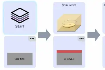
Although this shows only one transistor, these steps are performed on an entire wafer (eg. 100mm circular area), meaning each step is making 1000's of transistors are a time.

The main steps you can use are (not only in this specific order):

  • Patterning with Photolithography
  • Adding material with deposition or plating. Coats entire wafer.
  • Removing material with Etching. Removes only where photolithography has not protected.
  • Repeat some sequence of the above steps with different patterns and materials to build up the desired 3D structure.
Demis
  • 267
  • 1
  • 9