3

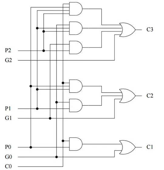
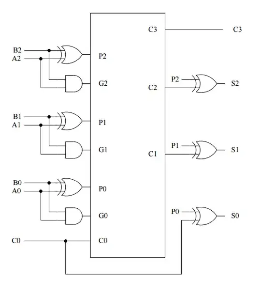
So I have to analyze this circuit, with inputs C0, A0, B0, A1, B1, A2 and B2, and outputs S0, S1, S2 and C3. It's been suggested I don't use a truth table to figure it out. I need to find out what the circuit does by deriving expressions for the outputs.

So far I've identified the XOR gate, and the AND gate sections for the A,B pairs, are adders. I am yet to figure out what the logic block is. By putting in values A=101, B=111, C0=0, I have found out that this whole system is an adder. But I don't know what the logic block section is. That's what I've done so far.Inputs and Outputs
Internal structure of the logic block

hazzey
  • 10,730
  • 11
  • 46
  • 96
kb2712
  • 31
  • 1

1 Answers1

2

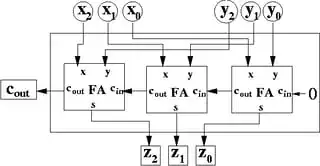
The circuit appears to be a ripple carry adder using full adders.

When compared to this circuit:

enter image description here

Image courtesy of this tutorial

You can see how the X and Y inputs map to your A & B inputs. The Z outputs map to your S outputs.

The input and output names give you a hint as to the circuit function as well. C0 implies an input carry bit from the previous adder. C3 implies an output carry bit, with C1 and C2 being used inside of the chip. S0 - S2 also imply a "sum" output of the input bits.