-1

I watched Ben Eater video on Youtube giving an introduction to tri state logic (https://m.youtube.com/watch?v=faAjse109Q8&t=98s).

He first presents a circuit made of two transistors (see picture)gate

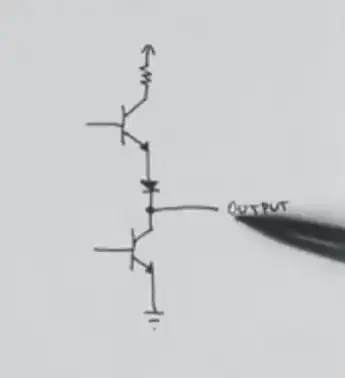
He shows that depending on whether the top or bottom transistor is on, the circuit will act as a current source or sink. Then he explains how this poses a problem with buses and the need of an enable pin.

He states that if both transistors are off, then the output is disconnected so it will not interfere with the bus. After that, he talks about using a specific chip for the job.

But I would like to understand how the enable pin actually works and how it can be implemented using low level electronic parts (transistors, resistors and the like).

How one effectively disconnect the output using a control signal? Does a simple transistor able to disconnect the output or is there more to tell about it?

I’m new to electronics so simple English answers will be appreciated.

Edit: if I plug the buffer input to the top transistor and plug the enable pin to the bottom transistor, will it do the job?

Winston
  • 281
  • 2
  • 10
  • 1
    Given both output devices are NPN, their bases will be clamped to Ground. – analogsystemsrf Aug 13 '19 at 09:11
  • This video made me a sad panda. ‘You know’ ... his explanation is pretty much fail. – hacktastical Aug 13 '19 at 09:12
  • @analogsystemsrf: you mean if both their bases are connected to low? How does that prevent from actually disconnecting the output? I thought current would not flow in the reverse direction in a transistor (like diodes). – Winston Aug 13 '19 at 09:21
  • 1
    @hacktastical: his explanation of what? The entire explanation (tristate, bus, etc) seemed ok to me, except the actual implementation of the enable pin. – Winston Aug 13 '19 at 09:22

3 Answers3

2

An internal schematic of a TTL tristate buffer can be found here: https://www.ti.com/lit/ds/symlink/sn54ls125a.pdf

The short answer is, the gate pre-drivers are shut off so the main drivers are held off too, leaving the output as high-Z. It’s complicated for a TTL output because this logic used only NPN type transistors, so they use all kinds of biasing tricks to make the output work as a push-pull.

Below is a simplified version of a 3-state totem-pole TTL device: enter image description here

The pre-driver T2 is a ‘phase splitter’ that generates complementary waveforms on its collector and emitter, effectively giving each output NPN opposite drive. In reality there would be another buffer before that input: buffer disable would not be grounding the input.

For CMOS it’s much simpler: series FETs are interposed between the driver sources and the supplies. Like this: enter image description here

hacktastical
  • 53,912
  • 2
  • 49
  • 152
  • Thanks. I downloaded this exact document after Justme mentioned it in their comment, and I certainly did not expect that amount of complexity. Why a simple solution such as feeding data to top transistor and enable signal to the bottom one in Ben Eater’s drawing not good enough? Does that mean that he is wrong and turning off both transistors will not disconnect the output? – Winston Aug 13 '19 at 09:00
  • No, it means that he probably also found the actual disabling method used inside real TTL ICs hard to explain. So he did the same hand-wave as the rest of us are doing, because we’re too lazy to fully reverse-engineer and analyze that jungle of a circuit. – hacktastical Aug 13 '19 at 09:06
  • Ok, this is a bit disappointing but apparently true. I came across "courses" on the internet like this one: – Winston Aug 13 '19 at 09:09
  • http://www.electronicsteacher.com/computer-architectures/digital-circuits/tri-state-logic.php – Winston Aug 13 '19 at 09:11
  • and it seems to me this "teacher" is fake as he says: When the enable input is 0, the outputs are completely disconnected from the rest of the circuit. It is as if there we had taken an ordinary circuit and added a switch on every output, such that the switch is open when enable is 0 and closed if enable is 1 like this: (picture of a switch in series) which is pretty close to the truth. The switch is just another transistor that can be added at a very small cost. (end of quote) Well, it has become clear another transistor will not suffice. Why though? You didn"t answer my question. – Winston Aug 13 '19 at 09:15
  • Because TTL is limited to NPN transistors only, and it’s not really feasible to make a series ‘transmission gate’ out of that device. So they do the next best thing: force the output drivers to be biased ‘off’. – hacktastical Aug 13 '19 at 09:20
  • Are you saying that other transistor types could offer another approach to this? And again, why feeding data and enable respectively to top and bottom transistor in Eater’s drawing will not work? – Winston Aug 13 '19 at 09:26
  • Thanks for mentioning a "transmission gate" by the way, I am reading about it, I didn’t know it. – Winston Aug 13 '19 at 09:29
  • I picked your revised answer. I would appreciate if you could explain why feeding data and enable respectively to top and bottom transistor in Eater’s drawing will not work. – Winston Aug 13 '19 at 09:41
  • It would work, based on the simplistic circuit I showed. That’s what D1 and D2 are doing. – hacktastical Aug 13 '19 at 09:49
1

With a normal push pull output, one of the output transistors is always on so output will be high or low. Basically with a three state buffer, the data input and enable input go through logic circuitry that makes a third state where both transistors are kept off.

Justme
  • 147,557
  • 4
  • 113
  • 291
  • But my question is how these transistors are kept off? I don’t suppose a mechanical relay is used. If by "logic circuitry" you say, rather quickly, some AND gate of sort will combine the enable and the input then this is not an answer at all because Ben Eater said gates either source or sink. So that’s back to square one if you use another logic gate unless you change something. – Winston Aug 13 '19 at 08:27
  • I should add high Z output is not a low output, it is disconnected. So it cannot be as simple as what you said. – Winston Aug 13 '19 at 08:30
  • Try Googling "tristate logic gate circuit" to see how it is done inside the chip. – user131342 Aug 13 '19 at 08:34
  • Since you specifically are interested in TTL circuitry, try to find SN74LS125A datasheet from Texas Instruments. It contains the internal schematics how the high and low side of the output driver is driven separately based on logic performed on data and enable signals. – Justme Aug 13 '19 at 08:36
  • Look in the TI databook for 54/74xx parts, using internal TTL logic to disable both source and sink transistors of the IC outputs was exactly how this was done. – hotpaw2 Aug 13 '19 at 08:41
  • Justme: I had Motorola SN54/74LS245 datasheet and it did not go into much detail, I checked Wkipedia too. Thank you for pointing to this TI datasheet, I checked it and it is very interesting and covers my question. I could not imagine it was so complicated though. What is the reason why a simple scheme like the one I mentioned in the edit of my question (last paragraph) will not work? And does that mean Prateek’s answer is wrong too? Thanks. – Winston Aug 13 '19 at 08:53
0

Tristate buffer

This is what a simple tri-state buffer looks like. In the diagram, X is the input, Y is the output and C is the enable with /C representing the negation of C. When the enable pin (C) is high, i.e. the buffer is enabled, the two transistors in the middle are ON and the device behaves like the above circuit by Ben Eater. When the enable pin (C) is low, i.e. the buffer is disabled and the transistors break all connections that may be made by turning the input on or off.

Prateek Dhanuka
  • 436
  • 3
  • 10
  • Thank you for the picture but I don’t see how inverted C break any connection when enable is low. Refering to your text it would seem both middle transistors should be controlled by C instead of being antagonistic...? – Winston Aug 13 '19 at 08:45
  • I'm pretty sure this is not how it's really done. That gate would have twice the output impedance of a normal one. – Dmitry Grigoryev Aug 13 '19 at 08:52
  • @Exocytosis, that is an N-MOSFET, it turns on when it is given a low voltage and turns off when given a high voltage. – Prateek Dhanuka Aug 13 '19 at 09:30
  • @DmitryGrigoryev, I didn't mean to say that this is how it's done. I thought it might be easier to understand this as an example. – Prateek Dhanuka Aug 13 '19 at 09:31
  • @Prateek: then your answer is irrelevant. I am asking about a real implementation, not a thought experiment. – Winston Aug 13 '19 at 09:37